In today’s smart device world, designers are faced with the challenge of adding wireless communication interfaces to their products. Whether you need to provide simple monitoring, data backhaul or product reconfiguration, the ability to add wireless device interfaces has become a requirement rather than an option. One technology found in many of today’s products is the FPGA (Field Programmable Gate Array). FPGA’s are becoming more prevalent in many products, but are rarely discussed when the conversation turns to adding smart device connectivity. In today’s post, I’ll discuss adding the SimpleLink™ multi-standard CC2650 wireless microcontroller (MCU) to your Altera Max10 FPGA Project. Although the target device in this post is Altera’s Max10 FPGA, the material is applicable to any Altera FPGA. For the following example we are using Arrow’s Max10 DECA board and, Arrow’s BeagleBone BLE / WiFi cape.
Let’s begin with an overview if the BLE / WiFi cape. The CC2650 wireless MCU shown below in GREEN, consists of the CC2650 device, a dedicated CJTAG programming header and a chip antenna. The CC2650 data interface can be accessed using either SPI or I2C. The programming header uses TI’s standard pin out, thus allowing the CC2650 wireless MCU to be configured by a number of programming sources including: TI’s RF-06, CC2650DK or IAR’s CJTAG programmer. Sixteen of the CC2650 device’s 31 IOs are present on the expansion headers. Both the SPI and I2C interfaces are available on the modules P1 header.
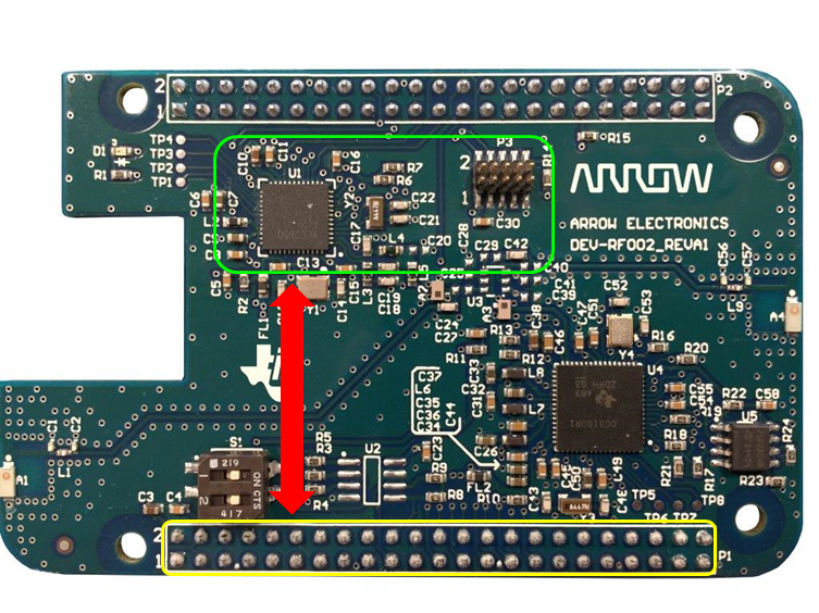 Figure 1: BeagleBone BLE / WIFI Cape
Below is the interface diagram for the DECA board and BeagleBone BLE/WIFI Cape. For today’s post we will focus on the SPI bus circled in RED. This bus is used as the primary communication interface between the Nios II soft processor and the CC2650 wireless MCU.
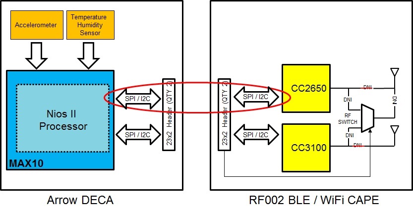
Figure 2: DECA to Cape Connection Diagram
The Nios II processor is synthesized from FPGA logic elements and resides inside the Max10 device. The function of the Nios II is to read the DECA’s onboard sensors and then transfer the sensor data to the CC2650 device. Upon receiving the sensor data, the CC2650 will transmit an update to the BLE connected device (smartphone or tablet). The CC2650 wireless MCU is configured to use a 500ms interval timer which sets the sensor update resolution. At every 500ms interval, the CC2650 device will strobe its data request signal. The data request signal is connected to a dedicated interrupt on the Nios II processor. Once interrupted, the Nios II will initiate a SPI data transfer and then request updated data from each of the DECA’s sensors. This will insure that updated sensor data is available at every 500ms interval.
For this design, we utilized Altera’s Nios II soft processor and a standard Qsys SPI peripheral. The Qsys system integration tool provides a convenient environment for building Nios II based systems. The figure below shows a portion of the system contents page which is used to manage the connectivity in a Qsys system.
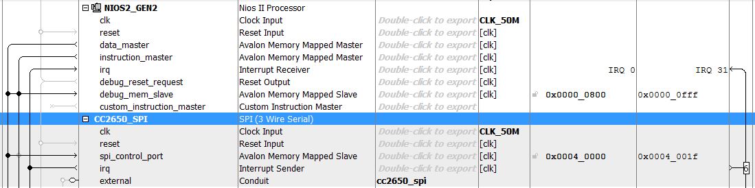
Figure 3: Altera’s Qsys peripheral list
In the figure above, you can see both the Nios II processor and the SPI peripheral. To connect the peripheral all you need to do is click on the bubble that attaches the SPI peripheral to the Nios II’s data_master and connect the SPI peripherals IRQ. The last step is to provide the peripheral with an address location and then configure the SPI peripheral itself.
The figure below shows the SPI peripherals parameter window. The parameter window provides all of the configurable attributes associated with the SPI peripheral, for instance clock rate, data width, shift direction etc.
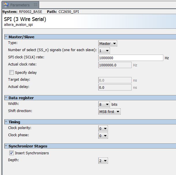
Figure 4: Altera’s Qsys SPI configuration window
Once you have completed adding all of your system’s peripherals you can generate your Nios II system. The output of the system generation process is an HDL (Hardware Description Language) module that can be instantiated in your FPGA design. You can select either VHDL or Verilog as the HDL output for the system generation process. In addition to the HDL module, the QSYS tool will also generate a nios.sopcinfo file that will be used to create a BSP (Board Support Package) for the Nios II software system.
With the hardware interface completed, all that remains is to add some software to read and write to the SPI peripheral. The Nios II software / firmware environment is an Eclipse based integrated development environment (IDE), so this should be familiar to most embedded designers. In Part 2 of our blog series, we will take a look at the embedded portion of our FPGA design.